Yes, SiC MOSFETs are susceptible to radiation. Silicon carbide’s wide bandgap, high critical electric field, and high-temperature performance make it attractive for spacecraft power conversion, but a commercial SiC MOSFET can still suffer threshold shifts, leakage degradation, gate damage, or catastrophic single-event burnout when energetic particles strike a biased device.
The most important lesson is that material robustness is not the same as radiation hardness. Device cell design, epitaxy, gate oxide, electric-field distribution, rated voltage, applied drain bias, temperature, particle species, energy, angle, and accumulated dose all influence the response. A part must be tested for the mission rather than accepted because it is made of SiC.
Why SiC is attractive for space power
Spacecraft increasingly use higher-voltage distribution, electric propulsion, compact converters, and electronics exposed to large temperature swings. SiC MOSFETs can reduce conduction and switching loss at high voltage, operate at higher junction temperature, and shrink magnetic and cooling hardware. These advantages can lower mass and improve efficiency.
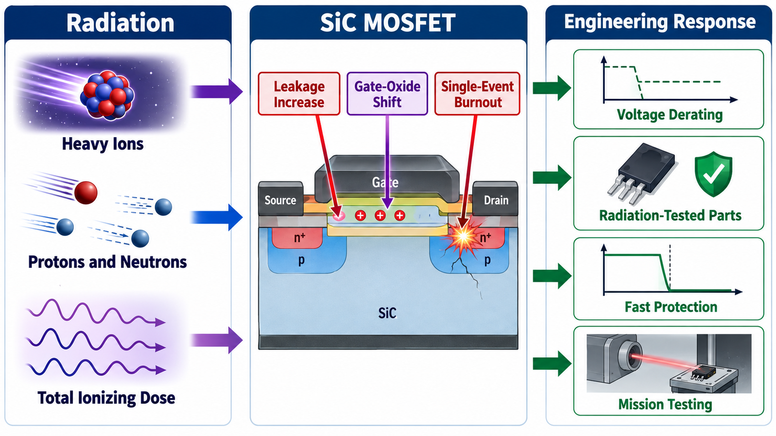
The same high electric field that enables compact high-voltage devices concentrates energy when a particle creates a dense ionization track. NASA testing has shown that heavy-ion strikes can produce permanent off-state leakage steps and single-event burnout at drain voltages well below the ordinary breakdown rating of some devices.
Single-event leakage current
A heavy ion passing through a biased off-state device generates electron-hole pairs along its track. The local electric field separates and multiplies charge. A noncatastrophic event can leave a small damaged region that permanently increases drain leakage. Repeated strikes may cause stepwise leakage growth.
This effect is often called single-event leakage current, or SELC. It matters even when the converter continues to operate because leakage changes standby loss, temperature, voltage sharing, and the device’s response to later radiation events. Test interpretation must distinguish temporary measurement noise from permanent degradation.
Single-event burnout
Single-event burnout is a destructive failure. The particle-induced current and electric field create localized heating and avalanche-like multiplication. If the generated energy cannot spread or be interrupted, a conductive path forms and the MOSFET fails, often short circuit.
Susceptibility rises with drain-source bias because a higher field gives the ion-generated carriers more energy. Some tested 1200 V SiC MOSFETs have shown burnout or degradation at a fraction of rated voltage. The exact threshold varies greatly by device generation and test conditions, so no universal derating percentage is safe.
Gate oxide and total ionizing dose
Total ionizing dose accumulates charge in the gate dielectric and at the SiC/oxide interface. Possible results include threshold-voltage shift, mobility change, increased leakage, altered transconductance, and reduced gate reliability. Bias during irradiation, oxide process, dose rate, annealing, and temperature affect the outcome.
SiC MOSFET gate interfaces already require careful control because interface traps reduce channel mobility and influence threshold stability. Radiation qualification should therefore include gate leakage, threshold, transfer curves, on-resistance, and time-dependent dielectric behavior, not only drain breakdown.
Protons and neutrons
Protons and neutrons can displace atoms and change material or interface properties. High-energy particles can also generate secondary ions through nuclear reactions, creating a localized track capable of triggering a single-event effect. The relevant spectrum depends on orbit, shielding, solar activity, mission duration, and planetary environment.
Shielding can reduce some lower-energy particles and total dose, but high-energy ions and secondary radiation can penetrate significant material. More shielding can add mass and can sometimes change the secondary-particle spectrum. Radiation transport analysis is needed before assuming that a thicker box solves the problem.
How radiation testing is performed
Heavy-ion testing exposes biased devices to particles with selected linear energy transfer, energy, fluence, and angle. Engineers monitor drain and gate current, detect degradation or burnout, and repeat at different drain voltages. Proton, neutron, and gamma or X-ray tests address other mechanisms.
The test board must limit fault energy without masking device response. Current compliance, cabling, decoupling, temperature, waveform monitoring, and post-irradiation measurements must be documented. Because leakage damage from one strike can affect later susceptibility, test sequence and stopping criteria matter.
Voltage derating
Reducing the applied drain voltage lowers electric field and can improve single-event margin, but the required derating is device- and mission-specific. Ordinary terrestrial derating rules do not replace radiation data. Use beam-test results for the exact part, preferably from multiple lots, and include uncertainty in the space environment model.
Derating also changes converter design. A lower usable fraction of rated voltage may require a higher-voltage part, more devices in series, a different topology, or a lower bus. Series devices introduce dynamic voltage sharing and gate-drive complexity. The article on high-voltage SiC gate-drive decisions describes related system constraints.
Circuit-level mitigation
- Use radiation-characterized parts: prefer data for the same manufacturer, part number, lot, bias, and temperature range.
- Limit fault energy: fuses, current limiting, fast isolation, and controlled DC-link capacitance can reduce secondary damage, though they may not save the struck die.
- Monitor leakage and temperature: trends can reveal cumulative degradation before a hard fault.
- Provide redundancy: a shorted power switch should not destroy every power channel or remove all critical loads.
- Control gate bias: keep VGS within qualified limits during normal operation, transients, radiation events, and unpowered states.
- Plan safe shutdown: protection logic should respond to overcurrent or desaturation quickly and avoid producing excessive drain overshoot.
Protection speed is limited by sensing delay, driver delay, gate discharge, and circuit inductance. A very fast turn-off can create destructive overshoot. Layout and gate control therefore remain important, as explained in SiC MOSFET negative-gate-bias design.
Are SiC MOSFETs better than silicon under radiation?
The answer depends on the radiation effect and device. SiC can offer better temperature and high-voltage power performance, and some parameters may tolerate dose well. However, NASA data have shown unexpectedly strong susceptibility of certain commercial SiC power devices to heavy-ion-induced leakage and burnout. A broad material comparison cannot replace device-level testing.
The decision should include efficiency, mass, thermal range, radiation response, fault mode, availability, screening, and qualification. For normal terrestrial reliability monitoring, see online ageing detection in SiC MOSFETs; radiation monitoring adds particle-specific mechanisms to that baseline.
Mission qualification workflow
- Define orbit or radiation environment, mission duration, shielding, temperature, and duty cycle.
- Translate the environment into TID, displacement damage, particle spectra, and single-event requirements.
- Select candidate parts with adequate electrical and thermal performance.
- Review public radiation data and identify gaps for the exact device generation.
- Test representative lots under realistic off-state bias, gate bias, temperature, and fluence.
- Measure leakage, threshold, RDS(on), gate current, switching behavior, and destructive thresholds before and after irradiation.
- Apply evidence-based voltage derating and fault-energy limits.
- Validate converter-level protection, redundancy, and end-of-life performance.
Radiation is only one reliability stress. Thermal cycling, vibration, gate-oxide aging, packaging, and switching overshoot still apply. The MOSFET thermal guide helps connect electrical loss to a temperature margin that radiation testing should preserve.
Frequently asked questions
Are SiC MOSFETs radiation hard?
Some devices or custom designs can be radiation tolerant, but commercial SiC MOSFETs should not be assumed radiation hard without relevant test data.
Can shielding prevent single-event burnout?
Shielding can reduce parts of the radiation environment, but energetic ions and secondary particles may remain. Device selection, derating, and system protection are still required.
Does a higher voltage rating guarantee better radiation margin?
No. Cell design and electric-field distribution matter, and different devices with the same rating can respond differently. Use measured single-event data.