A power MOSFET can conduct current through its enhanced channel in either direction, but a single device does not block both directions when it is off. The intrinsic body diode provides an uncontrolled path for one current polarity. This difference between conduction and blocking is the source of much confusion.
For an N-channel MOSFET used as a low-side switch, conventional load current normally flows from drain to source. If circuit conditions force reverse current and the gate is sufficiently positive relative to the source region, the channel can carry current in the opposite direction too.
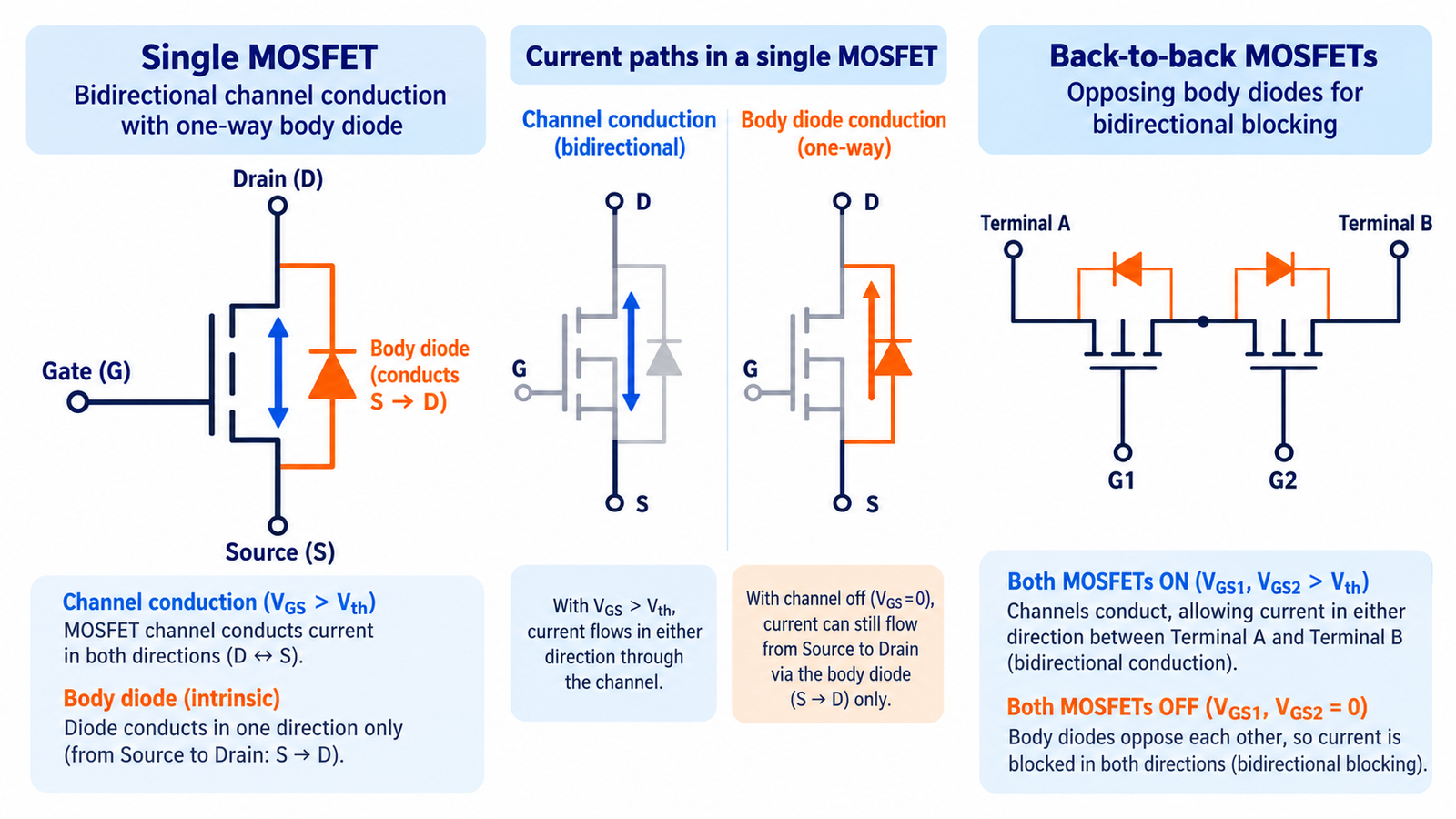
Channel current versus body-diode current
The enhanced channel behaves approximately as a resistance, so its current direction follows the applied drain-source voltage. With the gate off, the channel disappears, but the body diode remains. Reverse current may first forward-bias that diode; turning the channel on can then reduce the voltage drop by synchronous rectification.
The primer on MOSFET operation helps separate gate-controlled channel behavior from the diode built into a power structure.
Why source and drain still matter
Textbook symmetry is limited in a discrete power MOSFET. Its body is internally tied to the source, which establishes body-diode orientation and affects maximum ratings. Packages may provide a Kelvin source for the driver. Reverse transfer, capacitance, avalanche location, thermal path, and characterized switching performance all assume the data-sheet pin roles.
Do not flip a device merely because the on-state resistance seems symmetric. Confirm gate-driver reference and all fault paths.
What happens with the gate off
An off N-channel MOSFET normally blocks positive drain-to-source voltage until leakage or breakdown becomes relevant. If the source-side voltage rises enough above the drain, its body diode becomes forward biased. Therefore a single MOSFET used in a battery disconnect may still allow charging or discharging in the unwanted direction.
A P-channel device reverses the polarities, but the same one-diode limitation remains.
Use back-to-back MOSFETs for bidirectional blocking
Connect two MOSFETs in series with body diodes facing opposite directions. Common-source and common-drain arrangements are both used. When off, one diode blocks each polarity; when both gates are driven correctly, the two channels conduct in either direction. The total resistance is the sum of both hot on-resistances plus interconnect resistance.
This architecture appears in battery protection, hot-swap controllers, USB power paths, solid-state relays, and electronic fuses.
Reverse current in bridge converters
Synchronous bucks, motor bridges, and inverters frequently require reverse current. Dead time may force current through a body diode before the opposite channel turns on. The diode’s forward drop and reverse recovery then affect loss and overshoot. Some controllers support diode emulation at light load to prevent unwanted negative current.
Gate timing and damping should follow the MOSFET gate-resistor and EMI tradeoff.
Analyze every state, not only normal current
Draw current paths for power off, gate off, gate on, reverse battery, precharge, hot plug, inductive decay, short circuit, and controller brownout. Include ESD diodes and supply pins in the driver because they can create unexpected backfeed. Check which node the gate voltage is referenced to while current reverses.
Measure both VDS polarity and VGS at the device. A negative VDS does not automatically mean the MOSFET is misbehaving.
Turn the answer into a robust MOSFET design
For Do MOSFETs Conduct in Both Directions?, create an operating-state table before choosing a device or protection value. Include off, startup, steady on, PWM transitions, shutdown, reverse current, load connection, controller reset, brownout, open load, overload, and short circuit. For each state, write the expected VGS, VDS, current, duration, repetition, and starting temperature. This exposes short but severe events that an average-current calculation hides.
Next, compare the table with guaranteed data-sheet limits and characterized curves. Use voltage margin for supply tolerance and ringing; use RDS(on) at the actual gate voltage and hot junction; use total gate charge and Miller charge for driver sizing; and use DC or pulsed SOA for intervals where voltage and current coexist. Include package, PCB copper, interface material, airflow, connector, and source-return inductance in the model. A transistor cannot be evaluated separately from its commutation path and gate loop.
Build a staged test plan that begins with limited available energy. Capture gate-to-source voltage at the pins, drain-source voltage, current, and temperature while changing one stress at a time. Repeat enough cycles to reveal cumulative heating and recovery behavior. Define pass limits before looking at the waveform, preserve oscilloscope files, and record device lot, ambient, probe method, and firmware revision. If measured peaks approach an absolute maximum, redesign for margin rather than accepting the result because one prototype survived.
Practical validation checklist
Validate at the worst credible supply voltage, load current, switching frequency, ambient temperature, and fault condition. Measure gate-to-source voltage at the device pins, drain-to-source voltage with adequate bandwidth, current, case temperature, and—when power or pulses are significant—estimated junction temperature. Account for probe ground inductance and avoid interpreting ringing created by the measurement setup as circuit behavior.
Compare every result with the data-sheet safe operating area, absolute maximum ratings, transient thermal impedance, and temperature-dependent curves. Test startup, shutdown, load connection, stalled or shorted load, controller brownout, and repeated operation. The guides to reading MOSFET safe operating area and MOSFET thermal calculation provide useful companion checks.
Frequently asked questions
Does current normally flow from source to drain?
For an N-channel low-side switch, conventional load current normally flows drain to source; electron flow is opposite. Reverse channel current is also possible.
Can I use one MOSFET as a bidirectional switch?
It can conduct both ways when on, but its body diode prevents bidirectional off-state blocking.
Do two back-to-back MOSFETs double the voltage rating?
No. They enable opposite-polarity blocking; do not assume the voltage rating doubles or divides equally without analysis.
Is reverse channel conduction harmful?
Not inherently, but current, loss, body-diode commutation, gate drive, SOA, and transient ratings must remain within limits.