To drive a SiC MOSFET, use the gate voltage recommended for that exact device, choose a fast isolated driver with high common-mode transient immunity, connect the return to Kelvin source, minimize gate-loop inductance, and add protection that can detect and shut down a fault within the device’s short-circuit limit.
A SiC MOSFET is voltage controlled, but its fast edge rates make the gate circuit part of the power stage. Stray inductance can create gate overshoot, false turn-on, oscillation, and uneven current sharing. A driver that works with a silicon IGBT or superjunction MOSFET is not automatically suitable for SiC.
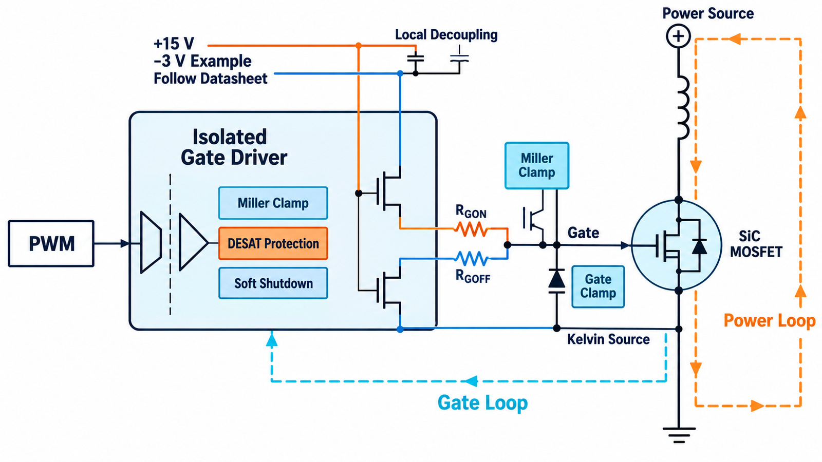
Start with the MOSFET datasheet
Read the recommended operating gate voltage, absolute maximum VGS, threshold range, gate charge, internal gate resistance, package source arrangement, and short-circuit information. Common examples use a positive turn-on voltage around 15 to 18 V and an off voltage from 0 to a few volts negative, but these values are not universal. Some newer devices have different recommended windows.
Leave margin between the nominal drive and the absolute gate rating for supply tolerance, ringing, and overshoot. A nominal voltage that is already near the maximum can become destructive at temperature or during a fast transition. The related article on whether an 800 V SiC MOSFET can be driven with 10 V explains why gate voltage must be matched to the device rather than inferred from drain rating.
Select the gate driver
The driver must source current to charge the gate and sink current to remove it. Peak current can be estimated from the gate-voltage step divided by total gate-loop resistance, while average gate-drive power is approximately switching frequency multiplied by gate charge and total voltage swing. Parallel devices multiply the required charge.
For a high-side or isolated power stage, check:
- Working and surge isolation voltage
- Common-mode transient immunity, or CMTI
- Peak source and sink current
- Propagation delay and channel-to-channel matching
- Undervoltage lockout thresholds for the intended bias rails
- Separate source and sink outputs or an external split-resistor network
- Active Miller clamp capability
- Desaturation or drain-voltage short-circuit detection
- Soft-shutdown behavior and fault reporting
Fast SiC half bridges can produce extremely high dV/dt. The isolation barrier must transmit the PWM command without a common-mode transient creating a false pulse. Choose the CMTI rating with margin above the measured switching-node slew rate.
Use the right isolated bias supply
The secondary-side bias supply powers the output stage of the isolated driver. It must maintain the positive and optional negative rails under switching load, meet isolation requirements, and have low coupling capacitance when common-mode current matters. Place local ceramic decoupling immediately between the driver supply pins and its Kelvin-source reference.
Negative turn-off bias improves false-turn-on immunity in a fast half bridge, but it increases gate-voltage swing and may affect third-quadrant conduction. A single-ended converter with a good layout may work reliably with 0 V turn-off. Review negative gate bias for SiC MOSFETs before adding a negative rail by habit.
Connect the Kelvin source correctly
A four-lead discrete device or module may provide a Kelvin-source or source-sense pin. Connect the driver return, gate clamp, and local bias decoupling to this pin. Carry load current through the separate power-source terminal. This prevents voltage across common-source inductance from appearing directly in the gate loop.
Do not join Kelvin source and power source far from the package. The benefit comes from keeping the drive reference separate until the device’s internal connection. Route gate and Kelvin source as a tight pair and keep them away from the switching node, transformer, and high-current commutation loop.
Minimize gate-loop inductance
Place the gate driver, turn-on resistor, turn-off resistor, clamp, and decoupling close to the MOSFET. Use short, wide traces or planes with small loop area. Avoid routing the gate trace over the drain switching node. Every connector or long lead adds inductance that weakens control of VGS.
Gate-loop inductance produces voltage equal to L multiplied by di/dt. During rapid gate-current change, only a few nanohenries can generate several volts of overshoot. That can exceed VGS limits or drive the device back on during turn-off.
Choose separate turn-on and turn-off resistance
A diode-and-resistor network or driver with separate outputs allows different RGON and RGOFF. Turn-on resistance controls current rise, drain-voltage fall, reverse-recovery interaction, overshoot, and EMI. Turn-off resistance controls voltage rise, current fall, ringing, and immunity to parasitic turn-on.
Begin with the device or evaluation-board recommendation, then measure the real double-pulse circuit. Include driver output resistance, internal gate resistance, and any ferrite impedance when estimating the total. The detailed tuning method in how to tune a MOSFET gate resistor for efficiency and EMI applies directly to SiC.
Prevent Miller-induced false turn-on
When the opposite switch changes voltage, current through the off-state MOSFET’s gate-drain capacitance can raise its gate voltage. If the bump crosses threshold, both switches may conduct at once. A strong sink path, negative off bias, low gate-loop inductance, separate turn-off resistor, and active Miller clamp reduce this risk.
An active Miller clamp should connect close to gate and Kelvin source. If long traces sit between clamp and device, their inductance prevents the clamp from controlling the actual gate voltage during the fastest interval.
Add fast short-circuit protection
SiC MOSFET short-circuit withstand time can be much shorter than that of an IGBT. Protection may use desaturation-like drain-voltage sensing, a current shunt, current transformer, or Rogowski sensor. The detection circuit needs a blanking interval that ignores normal turn-on ringing without delaying a real fault too long.
After detection, a controlled soft shutdown limits VDS overshoot caused by rapidly interrupting fault current. The total time from fault inception through detection, logic, propagation, and gate discharge must remain inside the verified device limit. The driver should latch the fault or enforce a safe retry policy defined by the system.
Clamp the gate without creating a poor loop
A gate-source TVS, Zener network, or dedicated clamp can limit positive and negative spikes. Select its working voltage, dynamic resistance, pulse capability, and capacitance so it protects the gate without interfering with normal drive. Place it next to gate and Kelvin source.
Do not rely on a clamp to correct a long, inductive layout. It can absorb the symptom while increasing gate current or oscillation. Reduce the loop first, then use the clamp as protection against remaining transients.
Measure the right waveforms
Measure VGS directly between gate and Kelvin source with a high-bandwidth probe and a very short connection. Measure VDS with a properly rated high-voltage differential probe and current with a sensor whose bandwidth and insertion inductance suit the test. Long oscilloscope ground leads can display ringing created by the probe itself and are dangerous on high-side nodes.
Use a double-pulse test to evaluate turn-on and turn-off at controlled bus voltage and current. Record VGS overshoot and undershoot, VDS overshoot, drain current, switching energy, delay, ringing frequency, diode recovery interaction, and temperature. Increase voltage and current gradually inside a protected test setup.
Parallel SiC MOSFETs carefully
Give each parallel MOSFET its own gate resistor. Make the power and gate paths symmetrical and match the Kelvin-source impedance. A shared driver avoids channel timing mismatch but must provide enough current. Separate drivers can sit closer to each device but need tightly matched delays and isolated supplies.
Static RDS(on) sharing does not guarantee dynamic sharing. Package inductance, threshold voltage, gate charge, and layout cause one device to switch first. Validate individual drain or source currents during the transient when possible.
Thermal and lifetime checks
Calculate conduction, switching, reverse-conduction, and gate-drive loss over the operating range. Fast switching may reduce transistor loss while increasing diode recovery, common-mode current, or magnetic loss. Check junction temperature using the correct transient or steady-state thermal model.
The guide to calculating MOSFET heat-sink size provides the basic thermal-resistance method. For a fast SiC module, include interface material, insulated substrate, baseplate, coolant, temperature cycling, and sensor placement.
Practical SiC gate-drive checklist
- Choose the MOSFET and record its recommended VGS window and absolute limits.
- Define bus voltage, peak current, switching frequency, topology, isolation, and fault requirements.
- Select a high-CMTI driver with adequate peak current, delay, UVLO, and protection.
- Design the isolated bias supply and local decoupling around the required rails.
- Connect driver return to Kelvin source and separate it from the power-source path.
- Place the driver, resistors, clamp, and decoupling next to the device.
- Implement independent turn-on and turn-off tuning.
- Add fault sensing, blanking, soft shutdown, and a defined latch or retry response.
- Validate with double-pulse testing before continuous operation.
- Check EMI, temperature, protection, and lifetime across component and environmental tolerance.
Frequently asked questions
Can I drive a SiC MOSFET with 10 V?
Only if the datasheet specifies acceptable performance at 10 V. Many devices require a higher positive gate voltage to reach rated low resistance, while newer generations may differ.
Is negative gate voltage always required?
No. It is useful for false-turn-on margin in fast half bridges, but 0 V turn-off can work in some devices and topologies with a good layout and strong sink path.
Why use Kelvin source?
It keeps load-current voltage across the power-source inductance out of the driver reference, improving control of the actual gate-to-source voltage.
Can one driver control several parallel MOSFETs?
Yes if it has sufficient current and the layout is symmetrical. Use an individual gate resistor for each MOSFET and validate dynamic current sharing.