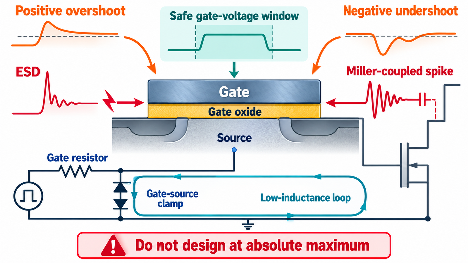
No. A power MOSFET should not be operated close to gate-oxide breakdown or its absolute maximum gate-to-source voltage in normal service. The absolute maximum is a damage boundary, not a guaranteed repetitive operating condition. Driver tolerance, supply variation, parasitic inductance, Miller current, switching-node dV/dt, and probe error can turn an apparently acceptable nominal voltage into destructive positive or negative spikes.
Use the manufacturer’s recommended on and off voltages, keep the gate loop compact, control ringing, and add a suitable gate-source clamp when analysis and measurement show it is needed.
What the VGS limit means
The gate is separated from the channel by a very thin dielectric. Excess electric field can create defects, leakage, threshold shift, or catastrophic rupture. A data-sheet absolute maximum such as ±20 V does not mean continuous operation at 19.9 V is reliable. Some technologies specify a narrower recommended drive range, and many SiC or GaN devices have different positive and negative limits.
Review how the MOSFET gate controls the channel to understand why almost no steady input current does not imply an indestructible gate.
Why gate voltage overshoots
The driver charges and discharges gate capacitances through resistance and loop inductance. A fast current change creates voltage across inductance. The resulting LC network can ring beyond the driver rails. Common-source inductance is especially troublesome because voltage in the shared source path changes the true VGS seen by the die while also feeding back into the driver loop.
Drain-voltage movement couples current through the gate-drain capacitance. During high dV/dt, that Miller current can lift an off gate or pull it negative, producing false turn-on or oxide stress.
Recommended drive, threshold, and margin
Threshold voltage is measured at a small current and is not the proper on-state drive. Choose a gate voltage that achieves the specified RDS(on) without approaching the limit. Include driver-supply tolerance, regulator startup, bootstrap behavior, transformer regulation, temperature, and component spread. For negative turn-off, remain above the specified negative limit in every transient.
A common engineering practice is to reserve substantial margin rather than operating at the boundary. The precise target must follow the device vendor’s data sheet and application guidance, not a universal percentage.
Control the gate loop before adding a clamp
Place the driver close to the MOSFET, use a dedicated Kelvin-source return when available, minimize loop area, and decouple the driver locally. Separate turn-on and turn-off resistors can control the two edges independently. A ferrite bead or carefully selected gate resistance may damp very high-frequency ringing, but excessive resistance increases switching loss and susceptibility to dV/dt turn-on.
The optimization process in tuning the gate resistor for efficiency and EMI shows how to change one parameter at a time and measure the result.
Use gate clamps correctly
A local gate-source Zener, TVS, or active Miller clamp can limit transients. It must clamp below the MOSFET limit yet above the intended drive over current and temperature. Place it at the device pins with a short path; a remote clamp leaves inductance between the gate and protection. Verify its pulse power, capacitance, leakage, tolerance, and failure behavior.
A clamp is not a substitute for a good layout. Repetitive clamp current indicates unresolved energy or coupling and can heat the device or clamp. The driver itself may include Miller clamping or split outputs that offer better control.
Measure the real gate-to-source voltage
Measure at the MOSFET gate and source pins, preferably using a low-capacitance differential probe and a very short connection. A long ground lead can create ringing that is not present—or hide ringing that is. Probe bandwidth, common-mode range, isolation, and placement must suit the switching node. Compare turn-on, turn-off, startup, shutdown, short circuit, and load-step cases.
For SiC-specific differences, consult how to drive a SiC MOSFET. SiC gate voltages and negative-bias recommendations vary by generation and manufacturer.
Reliability and fault cases
Repeated sub-catastrophic oxide stress can still degrade lifetime. Validate the hottest and coldest temperatures, maximum bus voltage, fastest device, strongest driver, minimum gate resistance, and worst layout. Analyze driver loss of supply, gate open circuit, shoot-through, desaturation or overcurrent response, and inductive turn-off. A short circuit can move source potential rapidly and stress the gate even when the driver rail is nominal.
The thermal consequences are covered in why MOSFETs get hot. Gate margin, drain-voltage margin, safe operating area, and junction temperature must all be satisfied together.
Design review questions for gate reliability
Ask what produces the highest positive and negative gate voltage, not only what the driver data sheet says. Review power-up sequencing, bootstrap refresh, isolated-bias overshoot, Miller current, fault turn-off, source-bounce, driver ground shift, and probe location. Confirm the gate resistor and clamp tolerances at temperature. If parallel MOSFETs are used, examine each gate separately because common and individual inductances can create different peaks.
Capture waveforms at minimum and maximum bus voltage, light and heavy load, hot and cold operation, startup, shutdown, pulse skipping, short circuit, and recovery. Overlay the measured extremes with the recommended drive range and absolute limits. Preserve sufficient margin for production variation and measurement uncertainty. Finally, inspect switching loss and temperature after any change that slows the edge. A modification that protects the oxide but drives the device through a long Miller plateau may move the failure mechanism from gate stress to excessive junction heat.
Frequently asked questions
Is ±20 V a recommended MOSFET gate voltage?
Usually it is an absolute maximum, not a recommended operating voltage. Use the drive range stated for the specific part.
Can a Zener protect the gate?
Yes, if its clamp voltage, tolerance, pulse capability, capacitance, temperature behavior, and placement are suitable. It does not replace a low-inductance layout.
Why can the gate go negative?
Gate-loop inductance, common-source inductance, transformer coupling, and drain dV/dt can pull the gate below the source during switching.
Where should VGS be measured?
Directly across the gate and source terminals with a short, appropriately rated differential measurement connection.