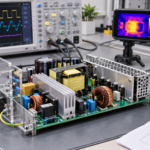
What is a switching power supply? A switching power supply, also called a switch-mode power supply or SMPS, converts electrical energy by turning semiconductor switches on and off at high frequency. Inductors, transformers, capacitors, and rectifiers transfer and filter that energy, while a control loop adjusts the switching pattern to keep the output voltage or current regulated.
Unlike a linear regulator, the main power transistor is intended to spend most of its time either off or fully on. That operating method can deliver high efficiency and high power density, but it introduces switching loss, electromagnetic interference, control-loop dynamics, and layout sensitivity.
How a switching power supply works
The exact circuit depends on whether the source is AC or DC, whether isolation is required, and whether the output must be lower, higher, inverted, or tightly regulated across a wide operating range. Most designs still contain the same functional stages:
- Input stage: accepts AC or DC and may include a fuse, surge protection, EMI filtering, and rectification.
- Power switch: a MOSFET, GaN transistor, or other semiconductor chops the input into controlled pulses.
- Energy-storage or isolation stage: an inductor or transformer stores and transfers energy.
- Output rectifier and filter: diodes or synchronous MOSFETs steer current while capacitors and inductors reduce ripple.
- Feedback and control: senses the output and adjusts duty cycle, frequency, phase, or pulse pattern.
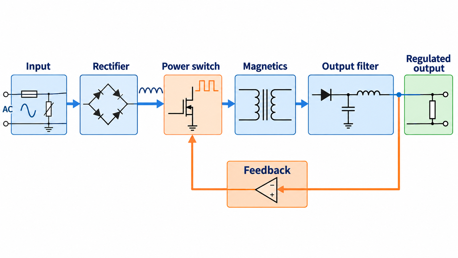
The site’s power-supply application section shows how this basic conversion chain supports adapters, charging, computing, communications, and other systems.
Why switching can be more efficient than linear regulation
A linear regulator controls output by dropping excess voltage across a pass device. Its approximate dissipation is the voltage drop multiplied by load current. When input voltage is much higher than output voltage, that heat can be substantial.
In an SMPS, a fully enhanced switch ideally has low voltage across it, while an off switch has nearly zero current. Real devices still lose energy through RDS(on), finite rise and fall time, output capacitance, gate charge, reverse recovery, magnetics, current sensing, and control power. Even so, well-designed switching converters often achieve much higher efficiency than a comparable linear solution.
Common switching-power-supply topologies
| Topology | Basic function | Typical use |
|---|---|---|
| Buck | Steps DC voltage down | Point-of-load rails, battery systems |
| Boost | Steps DC voltage up | LED drivers, PFC, battery interfaces |
| Buck-boost | Raises or lowers voltage | Wide-range battery-powered equipment |
| Flyback | Stores energy in coupled magnetics, often isolated | Adapters and auxiliary supplies |
| Forward | Transfers energy through a transformer while on | Moderate-power isolated supplies |
| Half bridge or full bridge | Alternately drives transformer or resonant tank | Higher-power isolated conversion |
| LLC resonant | Uses resonant current and soft switching | High-efficiency server, TV, and industrial supplies |
Topology is not chosen by name recognition. The decision follows from input range, outputs, isolation level, power, load behavior, hold-up time, regulation, cost, size, and compliance requirements. A compact power adapter and a kilowatt-class server supply solve different optimization problems even though both are switching supplies.
What the controller regulates
The controller compares a sensed output with a reference and changes the energy delivered per switching cycle. Pulse-width modulation varies duty cycle. Other converters vary frequency, peak current, phase shift, burst pattern, or a combination of controls.
Voltage-mode control directly adjusts the power-stage command from voltage error. Current-mode control adds an inner current signal that can simplify control behavior and provide cycle-by-cycle limiting. Digital controllers can implement calibration, telemetry, sequencing, and adaptive operating modes.
Isolation and feedback
An isolated supply uses a transformer and safety insulation to separate input and output circuits. Feedback may cross the barrier through an optocoupler, isolated amplifier, digital isolator, or an auxiliary winding and primary-side regulation method.
Isolation is a safety and system requirement, not merely a transformer symbol. Creepage, clearance, insulation system, transformer construction, protective earthing, fusing, and applicable product standards all affect the finished design.
Main components and what they do
- Power MOSFET or GaN switch: controls the input energy at high frequency.
- Gate driver: charges and discharges the switch gate with controlled timing.
- Inductor or transformer: stores energy, changes voltage or current, and may provide isolation.
- Rectifier: directs current to the output; it may be a diode or synchronous MOSFET.
- Capacitors: reduce input and output ripple and supply transient current.
- Controller: implements regulation, startup, limits, and protection.
- Sense network: measures voltage, current, and sometimes temperature.
At the AC input, a conventional bridge uses four diodes. The detailed explanation in how many diodes a bridge rectifier uses shows why two junctions contribute loss on each half-cycle.
Where switching-supply losses occur
Conduction loss
Current through MOSFET on-resistance, diode forward voltage, winding resistance, capacitor ESR, and PCB copper creates heat. RMS current is normally more useful than average current for these calculations.
Switching loss
Voltage and current overlap during transitions. Gate charge, output-capacitance energy, diode reverse recovery, dead time, leakage inductance, and ringing add loss. Raising switching frequency can shrink magnetics but increases several of these terms.
Magnetic and dielectric loss
Core material, flux swing, frequency, winding proximity effect, skin effect, and gap construction determine magnetic loss. Capacitor ripple current and dielectric behavior also contribute to temperature rise.
Standby consumption
The controller, startup network, bleeders, bias supplies, and burst-mode behavior determine no-load and light-load power. A converter optimized only at full load can perform poorly in real duty cycles.
Advantages of an SMPS
- High efficiency over a useful load range
- Smaller magnetics and filters at high frequency
- Ability to step voltage up, down, or invert it
- Practical galvanic isolation
- Multiple regulated or semi-regulated outputs
- High power density when thermal and EMI design are controlled
Wide-bandgap devices can push frequency and power density further, but the rest of the system must support their switching speed. The comparison of GaN and silicon in USB-C power adapters illustrates that device benefits depend on magnetics, control, layout, and thermal execution.
Disadvantages and design challenges
- Conducted and radiated EMI
- Fast voltage and current transients
- Control-loop stability requirements
- More components and design variables than a simple linear regulator
- Layout-dependent ringing, loss, and noise
- Safety and insulation work in offline designs
- Potential audible noise or burst-mode artifacts
How synchronous rectification improves efficiency
A synchronous rectifier replaces a diode with a controlled MOSFET. At low output voltage and high current, the MOSFET’s I × R voltage drop can be much smaller than a diode forward drop. Timing must prevent reverse current and cross-conduction. The design discussion in selecting MOSFETs for synchronous rectification covers conduction, gate charge, recovery, and dead-time trade-offs.
What to specify before choosing a topology
- Minimum, nominal, and maximum input voltage
- Output voltage, tolerance, current, and transient profile
- Isolation and safety requirements
- Efficiency targets at several load points
- Maximum ambient and component temperatures
- Size, height, airflow, and acoustic limits
- Ripple, noise, and EMI limits
- Startup, sequencing, hold-up, and fault behavior
- Expected life, qualification, and cost targets
This specification prevents topology selection from becoming a preference contest. It also exposes conflicts early, such as demanding very high switching frequency, extremely low standby power, wide input range, low cost, and minimal EMI filtering at the same time.
Verification checklist
- Measure efficiency and loss across line, load, temperature, and operating modes.
- Probe switch-node, gate, current, and output waveforms with suitable bandwidth and grounding.
- Check loop stability and transient response for the actual input and load range.
- Measure conducted and radiated emissions with representative cables and enclosure.
- Verify component temperatures after thermal equilibrium.
- Test startup, shutdown, brownout, short circuit, overload, and recovery.
- Confirm creepage, clearance, insulation, and protection against applicable standards.
Frequently asked questions
Is a switching power supply AC or DC?
It can be AC-DC, DC-DC, DC-AC, or AC-AC depending on the topology. The phrase describes the switching method, not one fixed input-output combination.
Is an SMPS always better than a linear supply?
No. An SMPS is usually favored for efficiency and conversion flexibility. A linear solution can be simpler and quieter for low-power, low-drop, or noise-sensitive stages. Many systems use both.
Why does a switching supply make noise?
Rapid voltage and current changes excite parasitic inductance and capacitance. Magnetics can also produce audible vibration. Layout, switching speed, snubbing, filtering, control mode, shielding, and mechanical construction determine the result.
What switching frequency is best?
There is no universal best value. Higher frequency can reduce passive size and improve transient bandwidth, but it can increase semiconductor, gate-drive, magnetic, and EMI loss. The optimum follows from the complete power-stage design.
Summary
A switching power supply regulates energy by rapidly operating semiconductor switches and controlling current through inductors or transformers. Its efficiency and power density come from minimizing time in high-loss states. A successful design balances topology, device behavior, magnetics, control, layout, EMI, thermal performance, protection, and safety rather than optimizing any one component in isolation.