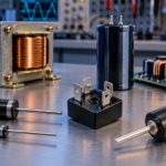
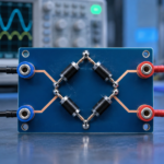
A Schottky diode is a rectifying semiconductor device built from a metal-semiconductor junction. It conducts mainly with majority carriers, so it typically has a lower forward voltage and much less stored charge than a conventional silicon p-n diode. Those properties make it useful in low-voltage rectifiers, high-frequency converters, clamping, polarity protection, and signal steering.
The advantages are not free. Reverse leakage is usually higher and rises strongly with temperature. Silicon Schottky devices also tend to cover lower blocking voltages than many p-n rectifiers. A correct design balances forward loss, reverse loss, voltage margin, surge capability, and thermal stability.
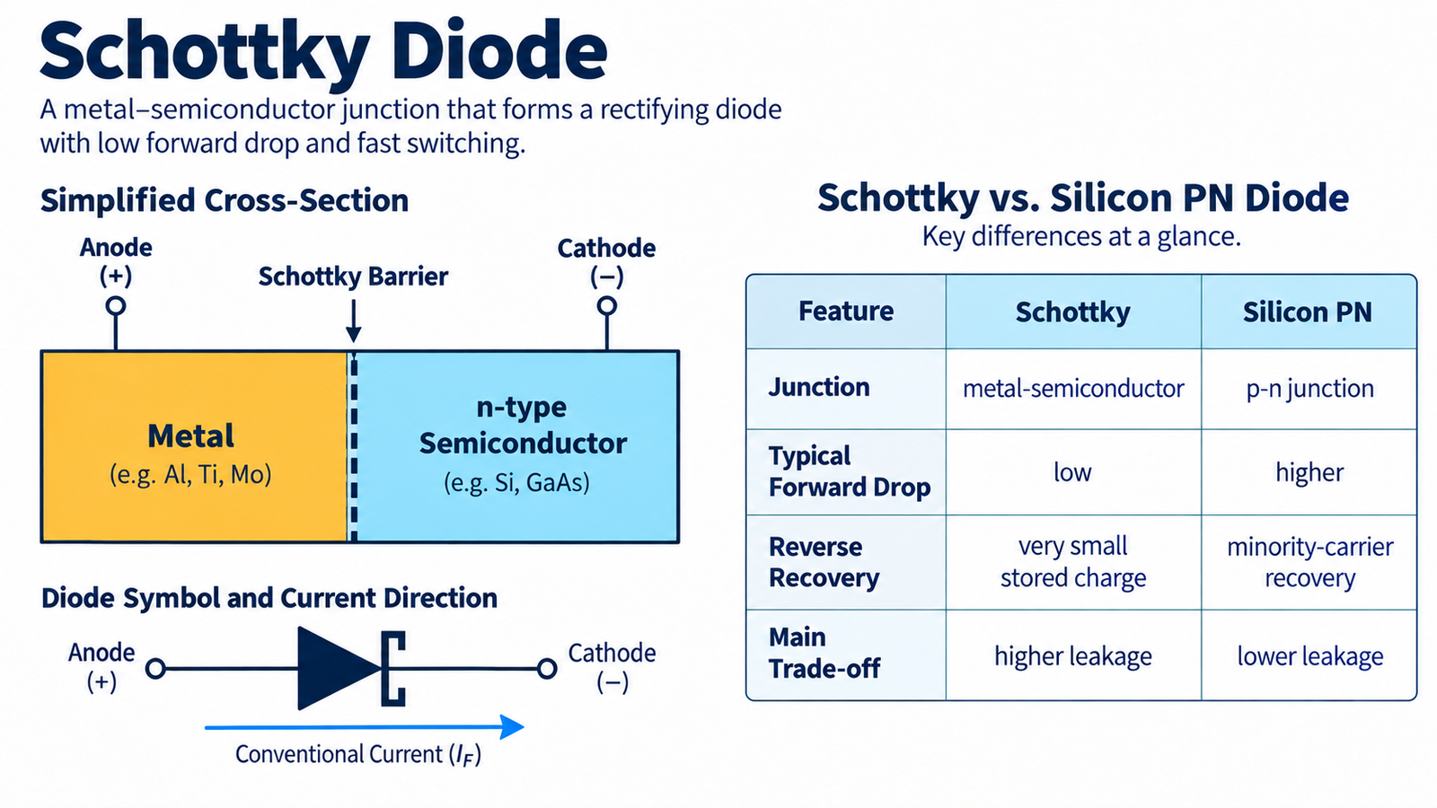
How does a Schottky diode work?
At the metal-semiconductor interface, the materials’ work functions create an energy barrier. With forward bias, majority carriers can cross the barrier and current increases. With reverse bias, the barrier blocks most current, although leakage remains.
A p-n diode injects and stores minority carriers during forward conduction. When the voltage reverses, that stored charge must be removed before the diode fully blocks. A Schottky diode largely avoids this minority-carrier storage. It can therefore commutate quickly, although junction capacitance and circuit parasitics still produce transient current.
Why is the forward voltage lower?
The barrier and carrier transport mechanism allow many silicon Schottky diodes to achieve a lower forward drop than comparable silicon p-n rectifiers. The exact VF is not one fixed value. It depends on forward current, junction temperature, die area, barrier design, and voltage rating.
Lower VF is especially valuable on low-voltage outputs. A 0.3 V or 0.5 V drop consumes a much larger fraction of a 3.3 V rail than of a 48 V rail. Approximate forward loss with Pforward = VF × IF(avg), then use datasheet curves at the expected current and temperature.
Schottky diode versus a standard silicon diode
| Characteristic | Schottky diode | Silicon p-n diode |
|---|---|---|
| Junction | Metal-semiconductor barrier | p-n semiconductor junction |
| Forward voltage | Usually lower for a comparable low-voltage device | Usually higher |
| Stored-charge recovery | Very small; capacitance still matters | Can have significant reverse-recovery charge |
| Reverse leakage | Generally higher and strongly temperature dependent | Generally lower |
| Typical use | Low-voltage, high-frequency rectification and clamping | General, high-voltage, ultrafast, or low-leakage rectification |
For a deeper look at commutation timing, read the site’s guide to optimizing dead time in synchronous rectification.
Common Schottky diode applications
- Switching power supplies: output rectification in buck, flyback, and forward converters, especially at low output voltage.
- Freewheeling paths: carrying inductor current while a switch is off.
- Reverse-polarity protection: a series diode is simple, although an ideal-diode MOSFET may waste less power at high current.
- OR-ing: isolating redundant supplies or multiple sources.
- Clamping: limiting a signal close to a rail because conduction begins at a relatively low voltage.
- RF detection and mixing: small-signal Schottky diodes can respond rapidly with low junction charge.
- Solar bypass: providing a current path around shaded cell groups, subject to careful thermal design.
Power rectification is a major use within a power supply, but the correct diode technology changes with voltage, frequency, current, and efficiency target.
Key datasheet parameters
Repetitive peak reverse voltage
VRRM must exceed the maximum repetitive reverse stress, including input tolerance, transformer leakage spikes, ringing, and load transients. Do not select only from nominal voltage.
Forward voltage
Compare VF at the actual current and temperature. A lower headline VF may come with higher reverse leakage. Use the curve and maximum limits rather than a single typical point.
Reverse leakage current
IR can grow by orders of magnitude as junction temperature rises. Reverse loss is approximately VR × IR during the blocking interval. In a hot design this loss can cancel the efficiency gained from lower VF.
Average and surge current
IF(AV) is thermal-condition dependent. IFSM describes a defined short surge waveform and cannot be treated as a repetitive current rating. Check startup capacitor charging and fault energy.
Junction capacitance
Capacitance creates displacement current during fast voltage transitions and can affect switching loss, ringing, and signal bandwidth. “No reverse recovery” does not mean zero dynamic current.
Thermal resistance and package
Confirm how heat flows through the leads, exposed pad, PCB copper, or heatsink. Package current and thermal limits may be reached before the silicon’s theoretical capability.
Thermal runaway risk
Reverse leakage increases with temperature. That leakage produces more reverse power, which raises temperature and can increase leakage again. If the cooling path cannot remove the extra heat, a positive feedback loop can cause thermal runaway.
Evaluate worst-case maximum leakage at the highest reverse voltage and temperature, not only room-temperature typical leakage. Include neighboring heat sources and reduced airflow. The detailed article on preventing thermal runaway in Schottky rectifiers gives a practical stability method.
Silicon versus SiC Schottky diodes
Silicon carbide Schottky barrier diodes extend majority-carrier rectification to much higher blocking voltages. They offer low stored-charge switching loss and strong high-temperature capability, but their forward-voltage behavior, cost, package, and application space differ from low-voltage silicon Schottky diodes. Compare technologies at the complete converter operating point rather than assuming one is universally better.
How to select a Schottky diode
- Determine maximum repetitive reverse voltage and transient overshoot.
- Calculate average, RMS, peak, and surge forward current.
- Estimate forward loss from VF curves at the hot operating point.
- Estimate reverse loss from maximum leakage at voltage and temperature.
- Include capacitance-related switching current and circuit ringing.
- Build the thermal path and calculate junction temperature with margin.
- Verify waveforms and temperature on hardware under worst-case conditions.
You can also browse the site’s diodes and rectifiers design articles for related selection and reliability topics.
Frequently asked questions
Is every low-forward-voltage diode a Schottky diode?
No. Other structures can be optimized for low forward drop. Confirm the device technology and dynamic behavior in the datasheet.
Does a Schottky diode have zero reverse recovery?
It has negligible minority-carrier stored charge compared with a p-n diode, but junction capacitance, package inductance, and circuit commutation still create transient current and loss.
Why does a Schottky diode fail short?
Possible causes include overtemperature, excessive reverse voltage, surge current, thermal runaway, poor soldering, or repetitive avalanche beyond its capability. Find the stress before installing a replacement.
Can I replace a standard diode with a Schottky diode?
Only if reverse-voltage margin, leakage, current, surge, capacitance, package, temperature, and certification requirements remain acceptable. A lower forward drop alone is insufficient.