Protect a MOSFET from dV/dt by limiting the drain-voltage slew rate where necessary and preventing Miller current from raising the off-state gate. The most effective measures are a compact gate loop, a low-inductance source reference, a strong turn-off path, separate turn-on and turn-off resistance, and an active Miller clamp or negative gate bias when the design needs more immunity.
dV/dt is not automatically harmful. Fast switching can reduce loss. The problem appears when parasitic capacitance and inductance convert that fast voltage change into unintended gate voltage, overshoot, common-mode current, or cross-conduction.
Understand the Miller-current path
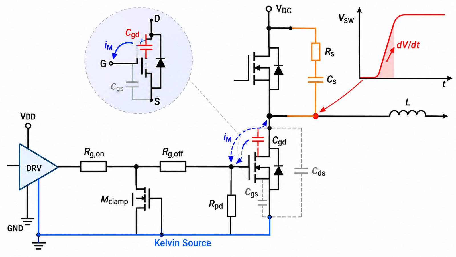
When drain voltage changes, current flows through the gate-drain capacitance CGD. That current must return through the gate resistor, driver output, source connection, and their parasitic inductance. The resulting voltage can lift the gate above threshold while the MOSFET should be off. In a half bridge, this creates shoot-through as the complementary switch turns on.
The exact risk depends on CRSS versus voltage, dV/dt, gate-loop impedance, threshold, temperature, and source bounce. The general gate behavior is reviewed in how a MOSFET works.
Fix gate and source layout first
Place the driver close to the MOSFET. Make the gate-out and source-return loop short and tightly coupled. Use a Kelvin-source pin or dedicated source trace when available so load current does not share the driver’s reference path. Put the driver bypass capacitor directly across its supply and return pins. Avoid vias and connectors in the gate loop unless the layout accounts for them.
Common-source inductance converts power-current di/dt into a voltage that changes the effective VGS. A larger gate resistor cannot fully correct a poor source reference.
Provide a strong controlled turn-off
A lower turn-off resistance gives Miller current a lower-impedance path to the driver. A diode and two-resistor network can set different turn-on and turn-off speeds. Select a driver with adequate sink current and low pull-down impedance at the actual gate voltage. Confirm that undervoltage lockout holds the gate off during supply ramp.
Too little resistance can create gate ringing and excessive current; too much can increase switching loss or allow false turn-on. The method in tuning a MOSFET gate resistor balances these effects with measurement.
Use Miller clamps and negative bias selectively
An active Miller clamp connects the gate to the local source with low impedance after turn-off. Place it close to the device. Some isolated drivers include a clamp; an external transistor clamp can also work when its loop is short. Negative off-state bias increases the voltage margin between the gate and threshold, especially for SiC or high-power IGBT stages.
Respect the device’s negative VGS limit and account for driver tolerance and ringing. A gate-source Zener or TVS can limit extremes, but its capacitance, dynamic behavior, and energy rating must fit the circuit.
Control the switching node itself
Reduce unnecessary drain overshoot and ringing with a compact commutation loop, local DC-link capacitance, controlled gate drive, and a correctly designed RC, RCD, or active snubber. Minimize switch-node copper area consistent with current and thermal needs because the node capacitively couples noise into heatsinks, chassis, transformers, and control circuits.
Slowing the active switch reduces dV/dt but increases transition energy. Tune at maximum bus voltage and current, then confirm light-load and soft-switching modes. Protection should not move the failure mechanism from false turn-on to overheating.
Protect sensing, isolation, and control paths
High dV/dt can create common-mode current through isolator capacitance, transformer interwinding capacitance, probes, heatsink pads, and PCB barriers. Select gate drivers and digital isolators with common-mode transient immunity above the measured edge rate with margin. Maintain creepage and clearance and keep sensitive traces away from the switch node.
Do not add large probe capacitance or long ground leads during validation. Use a differential or isolated probe rated for the common-mode voltage and bandwidth, and measure directly at the gate and Kelvin source pins.
Practical design review
Calculate approximate Miller current from effective CGD and dV/dt, but treat it as a screening estimate because capacitance is nonlinear. Simulate package and PCB parasitics, then validate the production layout. Capture off-state VGS, VDS, switch-node voltage, and leg current simultaneously where safe. Look for a gate bump aligned with the opposite device’s transition and for extra supply-current spikes that indicate cross-conduction.
Test maximum bus voltage, maximum current, minimum and maximum gate-driver supply, hot and cold devices, startup, shutdown, burst mode, short-circuit recovery, and external transients. Maintain margin to recommended gate limits, not merely absolute maximum. The caution in operating near gate-oxide breakdown explains why a clamp is only one layer of a reliable gate design.
Frequently asked questions
What is dV/dt induced turn-on?
It is unintended MOSFET conduction when a fast drain-voltage change sends current through gate-drain capacitance and raises VGS above threshold.
Does a gate-to-source resistor prevent false turn-on?
It helps define the off state, but at high dV/dt its resistance may be too high. A strong driver pull-down, clamp, Kelvin source, and good layout may also be required.
Should I always use negative gate bias?
No. It adds complexity and can violate negative VGS limits. Use it when the device, driver, and measured immunity requirements justify it.
Will a slower gate edge solve every dV/dt problem?
It may reduce coupling, overshoot, and EMI, but raises switching loss. Layout, driver impedance, clamping, and commutation-loop design should also be corrected.